Switching Power Supply Design Guidelines: Efficient PCB layout and wiring strategies
2024-06-05 14:17:32 1413
The printed circuit board (PCB) layout and routing design of the switching power supply is a key step to ensure the stable performance of the power supply, which is not only related to the correctness of the principle, but also directly affects the reliability, efficiency and electromagnetic compatibility (EMC) of the actual work. In this paper, INFINITECH will discuss in detail the important principles and specific practices of PCB layout and routing in combination with flyback converter design examples.
Basic principles of PCB layout and wiring
For the PCB layout and routing of the switching power supply is a very important link, not to say that the schematic diagram is correct, the subsequent work is not, in fact, the completion of the schematic design can only prove that the circuit principle is correct, and can not show that the circuit board designed according to this schematic can work normally. Because the reasonable layout and routing of the PCB will greatly affect the normal work of the circuit, such as the unreasonable layout of the PCB, the first thing that will be shown is the poor anti-interference ability of the circuit and the strong external radiation ability. For high-current switching power supplies, PCB layout mismatch causes the board to heat very seriously.
Therefore, PCB layout and wiring occupy a large part of the design of switching power supplies. This is especially true for PCB boards with high-speed signals. There are many rules for the layout of the switching power supply, which can be generally attributed to the high-power components on the top layer and the patch on the bottom layer; The line width of the high voltage line and the high current line should meet the requirements, preferably in the form of copper; The power loop and feedback loop should be small and the two should have a certain distance; There should be a certain interval between the components, and there should be a certain interval between the components and the PCB edge; The capacitor in parallel on the chip power supply pin should be as close as possible to the chip power supply pin and so on.
The following are some suggestions for the PCB layout of this design:
-
High-power component layout: High-power components are usually placed on the top layer, which helps to dissipate heat and reduces the effect of thermal stress on the circuit. The chip elements are arranged on the ground floor to optimize space utilization and reduce mutual interference between signals.
-
Line width and copper coating: For lines carrying large current or high voltage, the line width should be appropriately increased, and copper coating is ideally used to reduce resistance and temperature rise, and enhance anti-interference ability.
-
Loop minimization: The power loop and feedback loop should be as compact as possible and kept at a certain distance to reduce electromagnetic radiation and improve system stability.
-
Component spacing and edge distance: Ensure reasonable spacing between components and components to the edge of the PCB, which is conducive to heat dissipation and avoid interference caused by edge effects.
-
Bypass capacitor arrangement: The power pin adjacent to the power chip is connected in parallel to the patch capacitor to ensure a stable supply of power and reduce ripple.
For flyback converters, there are several points that need to be paid attention to when laying out and wiring, such as the input circuit part, the transformer part, the power chip part, and the feedback loop part. For the input circuit part, the input filter element should be spread in an area and leave some gaps between the components, and the line should be as wide as possible or directly walk the copper foil. The transformer part is an important source of electromagnetic interference, try to make the transformer close to the energy storage capacitor after the rectifier bridge, while the line is as wide as possible, from the energy storage capacitor to the transformer to the main switch tube and finally back to the energy storage capacitor this loop should be small, the sensitive line of the line as far away from this loop as possible. The concern of the power chip part is that the power pin of the chip should be connected with a chip capacitor to the ground pin of the chip. The placement of the chip capacitor should be close to the power pin of the chip. If it cannot be placed near the chip pin for some reason, it can also be placed on the back of the chip power pin.
Special considerations for flyback converters
-
Input circuit layout: Filter elements are centrally arranged, with appropriate gaps, and wide lines or copper foil are used to reduce input noise and improve immunity.
-
Transformer treatment: The transformer should be arranged close to the energy storage capacitor to ensure that the path of the large current loop is short, and the line width is increased to reduce electromagnetic interference.
-
Power chip design: The power pin bypass capacitors of the chip should be closely connected, and if they cannot be directly adjacent, they should be installed on the back to maintain the purity of the power supply.
-
Feedback loop optimization: The feedback signal line should be far away from the high-current and high-speed signal lines to ensure that the loop is small and well isolated to maintain stable output. Pay special attention to the routing of the optocoupler secondary to the power chip to ensure that the loop is compact.
The layout and wiring of the feedback loop is mainly concerned with the routing loop and the spacing between the high-current line. The signals above the feedback loop are important signals, which control the duty cycle of the output PWM wave of the power management chip to adjust the stability of the output. If the signal on the feedback loop is disturbed, it will inevitably affect the stability of the output. The wiring of the feedback loop should be far away from the wiring connected with the transformer, and away from the main switch tube. If there are large current wiring or high-speed signal wiring on the circuit board, the wiring of the feedback signal should also be far away from these wiring. The wiring of the feedback loop can be roughly divided into the wiring of the TL431 part and the secondary wiring of the optical coupling part. The TL431 is to take out the feedback signal, and the secondary of the optical coupling will react the feedback signal to the power management chip. In particular, the loop between the optocoupler secondary and the power chip is small.
Analysis of specific circuit examples
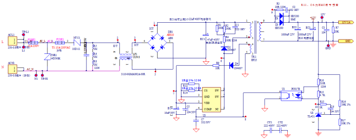
Figure 1 Overall schematic diagram of flyback power supply
Figure 1 After the switching power supply comes in from the mains live line L and the neutral line N, there is a safety tube with a large current, as shown in Figure 1. This is because there are other mains AC loads on the board, such as AC motors, which protect the circuit when the load current is too large. The current parameters of the fuse need to be calculated according to the actual load power. There is a varistor behind the fuse (as shown in Figure 2), which is used to suppress the surge and instantaneous peak voltage. When the voltage at both ends is higher than its threshold, the varistor value drops rapidly, thereby flowing a large current and protecting the rear circuit. After the varistor, there is a small current safety tube (as shown in Figure 2), which is the real overcurrent protection for the board switching power supply, preventing the power current from being too large and protecting the circuit.
The NTC resistance behind the fuse (as shown in Figure 2) is used to suppress the surge current when starting up, because the NTC temperature is low when starting up, the resistance value is large, and the suppression current is too large; When under the action of current, the temperature of NTC resistance rises, and the resistance value drops to a small amount, which does not affect the normal working current. The safety X capacitor (as shown in Figure 2) is used to filter out the differential mode interference of the mains, and the following three resistors are mainly used to discharge the X capacitor to meet the safety requirements and prevent the human hand from touching the metal terminal when cutting off the mains input. The reason for using multiple resistors is to spread out the withstand voltage and power. Common mode inductors (as shown in Figure 2) are used to filter out common mode interference currents.
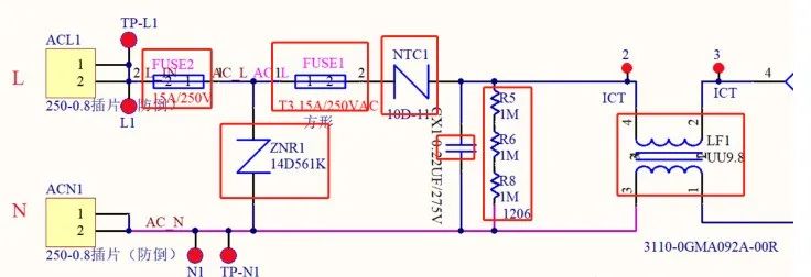
Figure 2 Input part of the circuit
EC1 has a general principle of 3uF/W in the industry, but it should be noted that the power is input power rather than output power. Assuming that the output power is 12W and the efficiency is 80%, the input power is 15W and the input capacitance is at least 45uF, as shown in Figure 8.
Since the flyback power supply evolved from Buck-Boost, its input loop and output loop are current discontinuous paths, so the smaller the control loop area, the better. The input capacitor EC1 should be close to the power chip, as shown in Figure 3. Similarly, the output rectifier diode and output capacitor should also be close to the transformer.

Figure 3
The RCD clamp circuit is used to absorb the Vds high voltage when the switch tube is turned off to prevent damage to the MOS tube (power chip). In Layout, the capacitor should be placed close to the transformer, followed by the resistor, as shown in Figure 4.
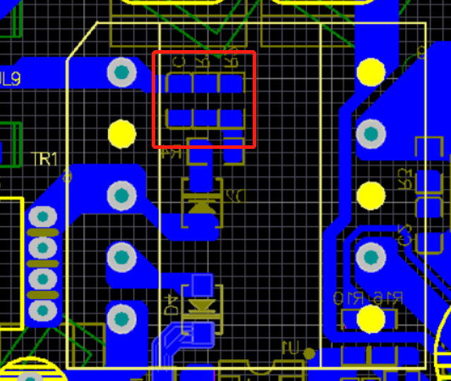
Figure 4
FIG. 4 Optocoupler is used for feedback output voltage and isolation. The Type II supplementary design schematic is referred to the above article and will not be repeated here. The primary GND of the optocoupler feedback loop should not be shared with the primary GND of the large current path, so as not to be affected by interference and cause output voltage fluctuation, so a single GND ground is pulled to the common ground of EC1 to form a single point grounding, as shown in Figure 5.

Figure 5
FIG. 5 RC RC absorption loops in parallel on both sides of the output rectifier diode are used to suppress EMI generated by the diode in the case of high frequency on-off, because the diode will produce voltage spikes (electric field) at the moment of on-off, and voltage spikes and current spikes (magnetic field) at the moment of off. Output capacitors EC2 and EC3 should pay attention to the current sharing design. As shown in Figure 6, the current path of the two capacitors is basically equal in length to avoid premature failure of a capacitor due to overcurrent.
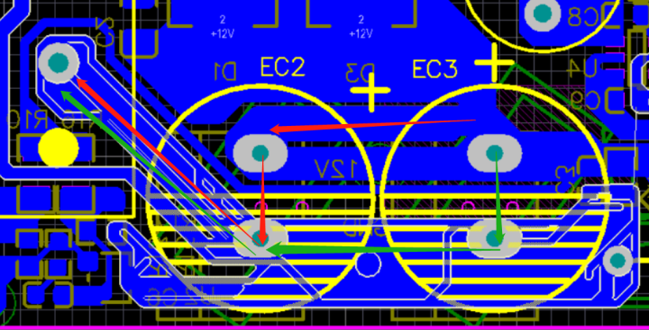 Figure 6
Figure 6 The output voltage feedback node needs to be removed from the end capacitor to improve the accuracy of voltage stabilization, as shown in Figure 7.
 Figure 7
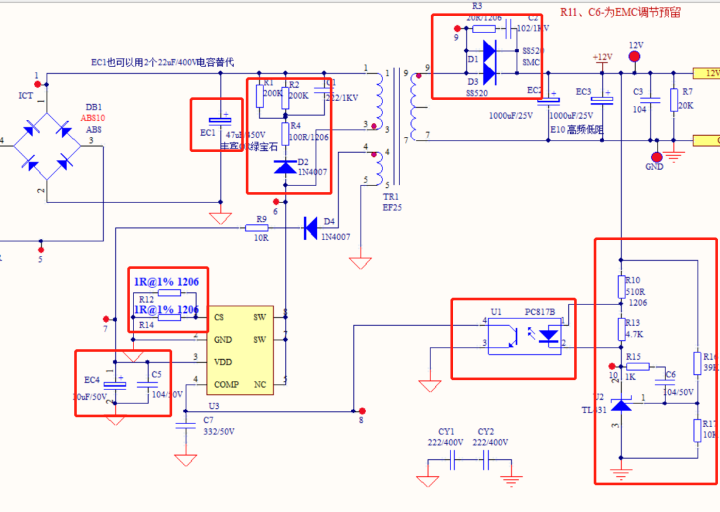 FIG. 8
It can be seen from the above analysis that PCB design of switching power supply is a meticulous and technically demanding work, and the optimization of every detail has an important impact on the performance of the final product. Following the above principles and adjusting flexibly according to specific application requirements is the key to realizing efficient, stable and low noise switching power supply.


